|
Professor David
F. Kelley
Professor
Ph.D., University of Washington
(1980)
Postdoctoral Fellow, Bell
Laboratories (1981-1982)
Email: dfkelley@ucmerced.edu
Office Phone: 209-228-4354
Selected
Publications
Postdoc position available: The group has recently entered into a new
collaborative research project with Nanosys Inc, and I am seeking a postdoc to work on this
project. Nanosys is located in Milpitas CA, and is a leading company involved in the development of Quantum
Dot (QD) technology for displays. See www.nanosysinc.com. This project is sponsored by a
academic/industrial grant from the U. S. Department of Energy and will
involve the development of new InP-based quantum dots for solid-state
lighting purposes. This application requires the development of QDs
that operate at high photon fluxes and elevated temperatures. Auger processes currently limit the
applicability of QDs at high fluxes and much of the research will involve
using ultrafast optical spectroscopy to elucidate how Auger processes can be
controlled by varying the QD morphology and structure. An application page on the UC Merced website is open, https://aprecruit.ucmerced.edu/JPF01109. Interested candidates can also email me directly.
This position has recently been
filled.
Physical Chemistry
Spectroscopy and dynamics of semiconductor nanoparticles. Dynamics of
condensed phase energy, electron and proton transfer reactions. Ultrafast
optical spectroscopy.
Research Overview
My research focuses on condensed phase spectroscopy and dynamics. We have
been particularly interested in the chemical, optical and electronic
properties of semiconductor nanoparticles and in electron transfer reactions
involving inorganic dyes.
Exciton dynamics in InP/ZnSe quantum dots.
InP/ZnSe QDs have many similarities and some profound
differences, compared to their CdSe-based counterparts. Two of the main differences are that InP is
less polar and has conduction and valence bans that are closer to the vacuum
level than CdSe. This affects several
aspects of the photophysics. One
aspect is the role that indium dopants in the ZnSe shell plays in the hole relaxation
rates. We recently showed that
following photoexcitation, the photoluminescence has a slow risetime,
indicative of very slow hole cooling in doped InP/ZnSe QDs.
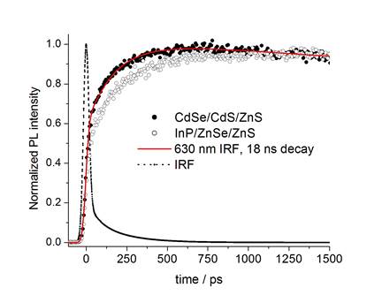
This is understood in terms of the energy levels of the
bands and the indium dopants, as shown in the figure below.
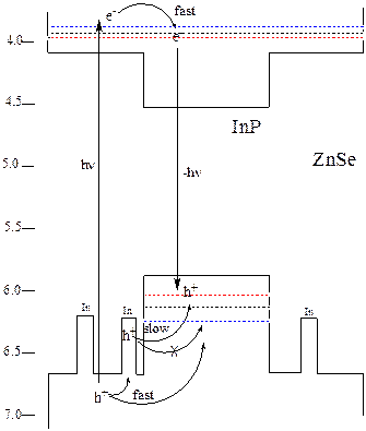
Energy level diagram and
trap-mediated slow hole cooling mechanism.
The calculated energies of the quantum confined electrons and holes
with respect to the vacuum level for the yellow (blue line), orange (black
line) and red (red line) QDs are indicated as dotted lines.
The role of these trap states in
the biexciton dynamics is currently under investigation.
Exciton dynamics in II-VI
quantum dots.
Surface states
can have a dramatic effect on the spectroscopy and photophysics of
semiconductor nanocrystals, also called quantum dots (QDs). The
effect of these surface states depends on the Fermi level – the energy of the
highest occupied state, as indicated in the figure, below.
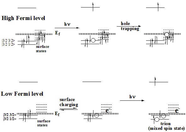
Our research group
has recently used transient absorption (TA) and time-resolved
photoluminescence (PL) spectroscopies to provide direct spectroscopic
evidence for the phenomenon of
thermal “surface charging” in II-VI (QDs).
We synthesize core/shell QDs with chalcogenide-rich surfaces, and
following ligand exchange with oleylamine, these QDs have empty low-lying
surface states that can be thermally populated from the valence band. At room temperature, the surface charging
equilibrium results in some fraction of the particles having a hole in the
valence band, i.e., the surface acceptor states make the particle
p-type. Photoexcitation of the surface
charged state results in what is essentially a positive trion, which can
undergo a fast Auger recombination.
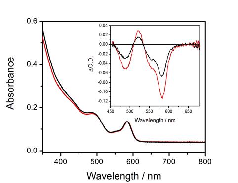
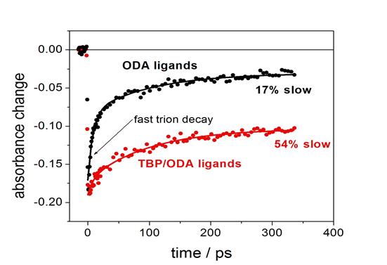
Both PL and TA (bleach recovery) kinetics of the CdSe/CdS QDs show a
70 ps decay component, which is assigned to Auger recombination of the
surface charged QD. The assignment is
established by the different amplitudes of the TA and PL decays.
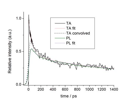
The empty
nonbonding surface orbitals can be passivated by ligation with a
trialkylphosphine, and the fast decay component is absent when
tributylphosphine is present. The
comparison of the TA and PL kinetics shows that the relative amplitude of the
70 ps component is a factor of about 1.5 greater in the TA than in the
PL. They also show that the fast
component in the PL spectrum is shifted about 6 nm to the blue of the exciton
luminescence.
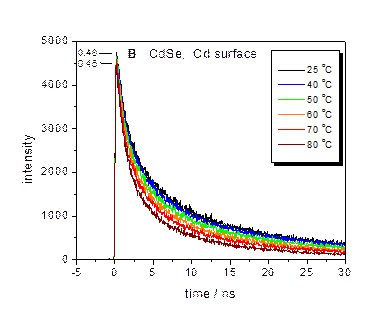
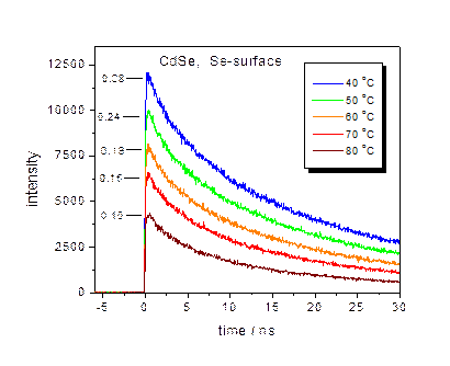
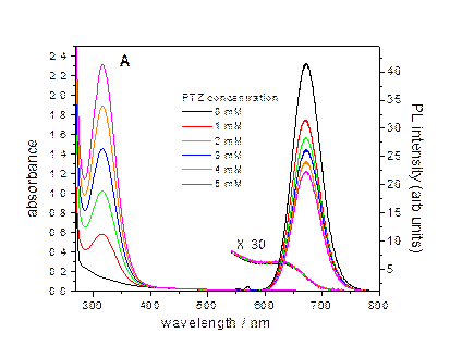
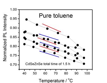
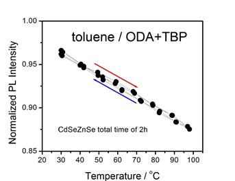
The presence of surface charging can result in “thermal quenching” of
the QD luminescence with a Se-rich surface, as shown below. Temperature dependent PL decay curves and
fractions of bright particles are indicated for CdSe (left) and
CdTe/CdSe/ZnSe (right). This
thermal quenching is due to an Auger mechanism, as given below.
  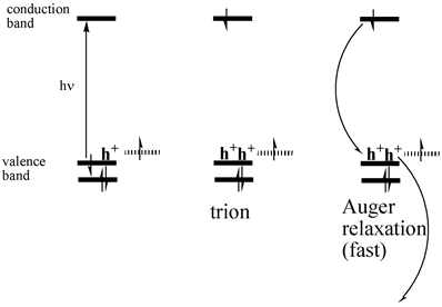
The important points are:
Photoexcitation of charged particles produces
“trions” (two holes and one electron) which undergo rapid radiationless
decay.
Trion formation is minimized by surface
derivitization of core/shell particles which eliminates the empty (electron
accepting) orbitals.
Thermal population of these orbitals follows
Arrhenius behavior, as plotted below.
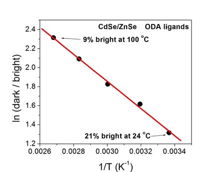 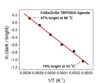
We find
that amines passivate the surface and eliminate the surface charging.

The amine and tributyl phosphine
ligands are stable up to about 80 °C.
Spectroscopy and morphology of core/shell
nanoparticles.
Lattice mismatch play a central role in determining the morphology and
the spectroscopy of core shell particles. In the present studies, we
examine the role of lattice mismatch in determining the shell uniformity in
core/shell nanocrystals.
Basic idea: If one starts with a
semiconductor nanocrystal and grows a shell of a different semiconductor
having the same crystal structure but a different lattice constant, then
there is a lattice mismatch at the core-shell interface. The strain
energy associated with the lattice mismatch increases with shell thickness,
but can be minimized by the formation of “islands”, rather than a continuous
shell of uniform thickness. Island formation increases the surface area
and therefore the surface energy. The morphology of the shell (the
uniformity of the shell thickness) is therefore a trade-off between strain
energy and surface energy. The distribution of shell thicknesses is
measured by measuring the distribution of charge tunneling times through the
shell (a very sensitive measure of shell thickness). To summarize,
Surface energy—proportional to surface area and controlled by the types of
surface-adsorbed ligands.
Strain energy—controlled by the radial composition profile—calculated through
elastic continuum theory.
Shell thicknesses—determined by measuring the rate of charge tunneling
through the shell.
The model system we have most extensively studied is
ZnTe/CdSe. This is a type-II system, similar to the extensively studied
CdTe/CdSe system. However, ZnTe and CdSe have nearly identical lattice
parameters. But, upon annealing, the cations diffuse and one gets a
particle best described as (Zn,Cd)Te/(Cd,Zn)Se, which has a large lattice
mismatch. The lattice mismatch and energetics of CdTe/CdSe and ZnTe/CdSe
particles are depicted below.
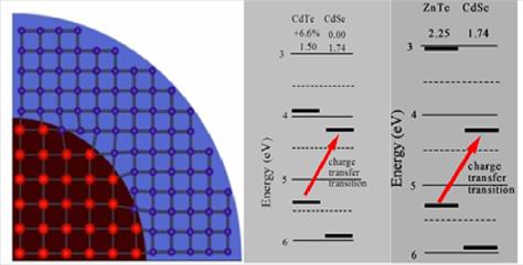
For ZnTe/CdSe zincblende nanocrystals, the we reach the
following conclusions: low temperature (200 °C) shell growth → very
little cation diffusion → relatively small lattice mismatch → uniform shell
growth to about a thickness of three CdSe monolayers (a wetting layer),
followed by island formation (Stranski-Krastanov growth). Shell annealing at
250 °C → extensive cation diffusion → larger lattice mismatch → island
formation w/o wetting layer (Volmer-Weber growth).
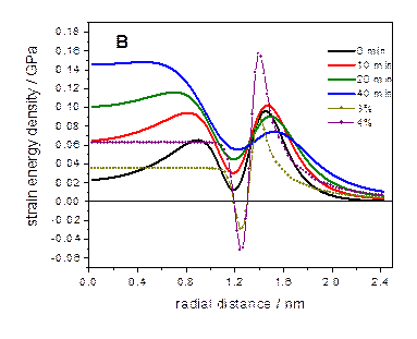
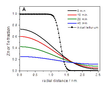
When a hole acceptor
(phenothiazine) is adsorbed on the particles surface, the charge tunneling
dynamics, and hence quenching kinetics are a very sensitive probe to the
local shell thickness. Dramatically different hole quenching kinetics
are associated with a smooth wetting layer (below, left) and
Stranski-Krastanov island growth (below, right). By analyzing the
luminescence decay, the shell thickness inhomogeneity (the shell surface roughness)
can be obtained. The calculated curves correspond to a Poisson
distribution of acceptors adsorbed on the particles at different
phenothiazine concentrations.
Lattice strain: elastic continuum
calculations.
The lattice strain energy can be calculated using elastic
continuum theory. It is the strain energy compared to the surface
energy that controls the shell morphology. For a finite shell with
inner radius rc and outer
radius R, the radial displacement in the shell is given by
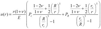 where E is Young’s modulus and n is Poisson’s ratio. where E is Young’s modulus and n is Poisson’s ratio.
Lattice coherency requires
The radial pressure is
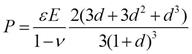 where e
is the ratio of lattice parameters and d is the ratio of shell
thickness to core radius. The core is under hydrostatic pressure. The shell
is under radial pressure and tangential tension. The core pressures are very
large, and can be more than 109 Pa. where e
is the ratio of lattice parameters and d is the ratio of shell
thickness to core radius. The core is under hydrostatic pressure. The shell
is under radial pressure and tangential tension. The core pressures are very
large, and can be more than 109 Pa.
The radial and tangential strains are given by
The radial and tangential stresses and strain energy
density are given by

The surface energy is difficult
to quantify, but is taken to be proportional to the surface area. 
Two-dimensional
CdSe Nanoplatelets
The exciton in spherical QDs
extends over the entire sphere.
However, in extended CdSe nanoplatelets (NPLs) this may not be the
case. The spatial extents of NPL
excitons are investigated using transient absorption (TA) spectroscopy. The bleach magnitudes of a series of NPLs
with varying lateral dimensions are compared with a quantum dot (QD)
standard, allowing the relative magnitude of the heavy hole (HH) bleach to be
determined as a function of size. The relative bleach of the HH absorbance
decreases with increasing NPL area, while the excitonic sizes calculated from
the bleach magnitudes are found to be independent of the lateral dimensions.
This result is consistent with a model that considers the relative
intensities of photoinduced absorption (PA) and stimulated emission (SE)
contributed by distinct regions of the platelet occupied by either the
electron, the electron and hole, or neither. Using this model gives an
average excitonic area of 21.2 ± 2.5 nm2.
Considering
the small spatial extent of the relaxed NPL exciton compared with the number
of oscillators participating in ground state absorption partially accounts for the discrepancy
between the HH extinction coefficients and the slow radiative rates, which
deviate from the values calculated from the Einstein relations by a factor
between ~ 30 – 80. The electron-hole overlap integral is estimated from the
ratio of HH bleach magnitudes before and after trapping the hole by
4-methylbenzenethiol (MBT), a hole acceptor, and is then factored into
calculations of the radiative lifetimes. Together with the measured
singlet-triplet splitting and e-h overlap, these considerations allow the NPL
radiative kinetics to be semiquantitatively reproduced.
Two-dimensional
GaSe semiconductor nanoparticles.
Many types of
semiconductors have properties which are particle size dependent.
Semiconductor nanoparticles are particles which are sufficiently small that
their physical and chemical properties are very different from those of bulk
materials, and are dominated by quantum mechanical effects, so-called
"quantum confinement". These particles are thus often referred to
as "quantum dots." We have been interested in semiconductor
nanoparticles because of their possible applications in regenerative
photocells, photocatalysis and in electroluminescent devices. Development of
quantum dots for all of these potential applications requires that we
understand their size-dependent spectroscopy and photophysics. We have been
primarily interested in the extremely photostable, two dimensional metal
dichalcogenide semiconductors, such as GaSe and InSe. The crystal structure
of bulk GaSe is shown
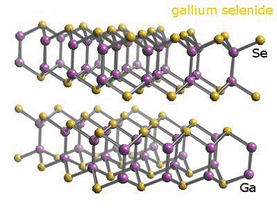
GaSe nanoparticles consist of "single tetra-layers", i.e., a single
sheet of covalently bound Se-Ga-Ga-Se. These particles have diameters ranging
from 2.5 to 10 nm and single sizes can be produced by controlling the
synthetic chemical environment.
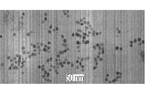 
TEM
images of 8.4 +/- .7 nm GaSe nanoparticles.
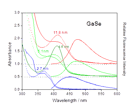
GaSe Nanoparticles: 2.7 nm – blue, 5.1 nm – light green,
4.6 nm - highly aggregated –
dark green
11.8
nm - red: “focused” distribution synthesized by multiple injections.
Aggregate
absorption spectra are dotted lines – monomers are solid lines
Photoexcitation of these particles produces
conduction band electrons and valence band holes. A major pathway following
photoexcitation is radiative decay, and the particles are strongly
luminescent.
The electrons and holes and undergo interfacial
charge transfer and/or trapping into localized surface states. One of the
main goals of the research have been to understand the optical spectroscopy
of these particles. We also use time-resolved ultrafast absorption and
emission spectroscopy to study electron transfer across the
nanoparticle/nanoparticle and nanoparticle/liquid interfaces. We have shown
that these nanoparticles form extended, somewhat disordered one dimensional
aggregates. This type of behavior is unique among semiconductor nanoparticles
and is due to their two dimensional, disk-like shapes; they form stacks in
room temperature solutions.
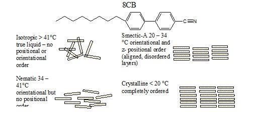
Nanoparticles
in liquid crystals.
Recently, we
have been putting GaSe nanoparticles in organic liquid crystals.
Specifically, GaSe nanoparticles are able to form a hybrid
organic/semiconductor liquid crystal with the smectic-A phase of 4-octyl,
4’-cyano biphenyl, 8CB. This is a common liquid crystal molecule , and the
phases of 8CB are shown below.
Incorporation of GaSe nanoparticles into the
liquid crystal results in almost complete alignment of the particles – the particle’s
normal line up with the liquid crystal director axis. This is seen from
static polarized absorption measurements, below. The “order parameter” (0 =
random orientations, 1= completely ordered) for these particles is about
0.96.
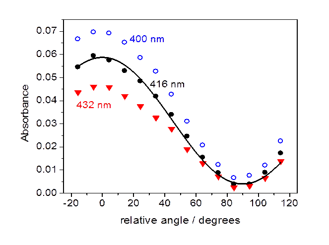
Absorbance
at several wavelengths as a function of the angle between the polarization of
the light
and
the liquid crystal director axis. Absorbances for 400 nm (open blue circles),
416 nm (solid black circles),
and
432 nm (solid red triangles) are shown. Also shown is a sine squared fit to
the 416 nm absorbances.
Thus, the particles form
well-ordered one-dimensional arrays in the liquid crystal host – the
disk-like particles stack like Frisbees or dinner plates. The lack of
disorder greatly increases the extent of particle-particle interactions, and
fluorescence from these nanoparticle arrays is shifted about 50 nm to the red
of that from solution phase GaSe nanoparticles. Time resolved results indicate that the
excitons travel large distances, at least microns!
|